Vacancy-Nitrogen Centers in Graphene for Qubits and Vacancy-Nitrogen Linear Arrays for Quantum Data Transfer
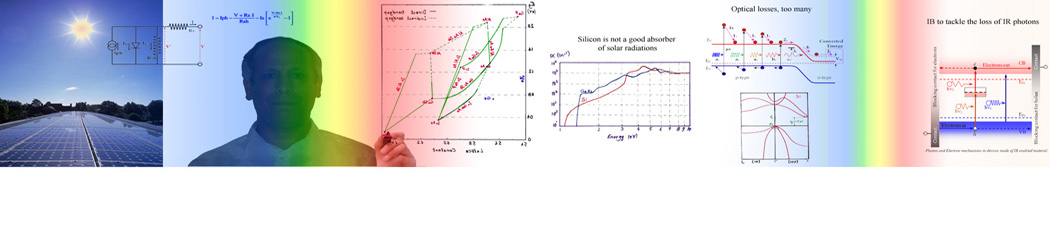
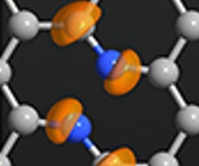
Goals: A new method for generating in a controlled fashion vacancies and vacancy arrays in graphene sheet has been discovered by Sahtout and Karoui. The vacancies are doped with nitrogen to create NV centers, which are useful for many applications: quantum devices, high efficiency catalyst,... Some of our goals is to understand the properties of these centers as single quantum entity or ordered array of the same, and to provide means to use them as elements for quantum devices. Pairs of NV complexes appear to be promising for making interesting bistable quantum systems, useful for instance for qubits. Furthermore, Karoui and Sahtout proposed that the intrinsic and doped vacancy lines can be used in quantum circuits for data transfer.
Chemical Sensors Operating at the Quantum Frontiers
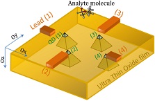
Goals: Understanding sensing functionalities useful for developing extremely sensitive gas nanosensors that are capable of detecting extremely small traces of highly toxic gases, such as organophosphates, in particular the lethal sarin, and provide the essential elements for designing such sensors.
Ordered Quantum Dot Arrays
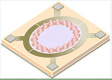
Goal: Study the physics of Ordered Quantum Dot Arrays for Quantum Information and Nanosensors.
Research on ordered quantum dot (QD) arrays is moving to revolutionize future engineering fields, including optoelectronics, third generation solar cells and beyond, bioengineering, and nanomedicine, to name a few. We have a strong interest in theoretically deriving the properties of QD arrays, the electron and photon confinement in such quantum systems, and charge carrier transport intra- and out of- QD arrays. Understanding the mechanisms of photons and charge carriers in these systems is essential for developing high performance optoelectronic and quantum computing nanodevices.
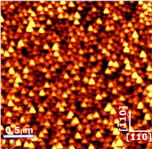
Fabrication of SiGe Quantum Dots for Third Generation Solar Cells and Characterization
Goal: Fabrication of layers of dense and uniformly distributed Quantum Dots (QDs) for Third Generation Solar Cells and IR Nanosensors, using low cost deposition technique.
Silicon-germanium nanodots are highly interesting for a wide range of applications including, but not limited to, photovoltaics, optoelectronic devices, nanosensors, high speed devices, integrated optoelectronic circuits, and quantum computing devices. We have fabricated using Rapid Thermal-Chemical Vapor (RT-CVD) SiGe nanodot layers for third generation solar cells. The nanodot layers were grown on solar grade silicon wafers. The focus was on engineering the dot size and distribution to increase IR photon harvesting. RT-CVD was chosen for it allows inducing growth conditions for nanodot self-assembling. In addition, it is a viable technology for photovoltaics for it allows deposition of large surface nanolayers at low thermal budget and at a low cost per unit area. Moreover, it offers flexibility on fabrication parameters.
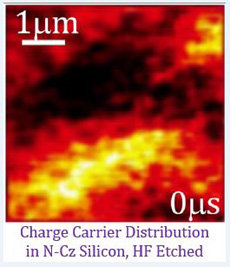
Dynamics of photogenerated carriers at the nanoscale
Goal: Nanoscale characterization of Semiconductor nanomaterials for Advanced Solar Cells and Nano-optoelectronic devices.
To understand the dynamics of photogeneration of charge carriers, and to help the design of third generation nanostructured silicon solar cells, we have carried out pioneering work on the measurement and analysis of charge carrier recombination and the effects of submicron scale stress inhomogeneity in silicon at the nanoscale.
- 1.b.05. Identification of Atomic Cluster Defects in Silicon through First Principle Calculations and IR Absorption Lines
- 1.b.06. Defect Nucleation during Silicon Crystal Growth: Theory and Experimental Validation of Point Defect Generation, Interaction, Transport, and Clustering
- 1.b.07. Control of Extremely Low Concentration of Impurities in Silicon Wafers
- 1.b.08. Fabrication and Characterization of Porous Materials for Sensors and Solar Cells
- 1.b.09. Characterization and Modeling of Defects in Polycrystalline Silicon.